- Stage of development
-
Validated prototype
- Intellectual property
-
Priority patent application
- Intended collaboration
-
Licensing and/or co-development
- Contact
-
Eva GabaldónVice-presidency for Innovation and Transfereva.gabaldon@csic.escomercializacion@csic.es
- Reference
-
CSIC/EG/126
Additional information
#Electronics
#Chips / Circuits / Micro & nanoelectronics
Power splitter for integrated photonic circuits
Ultra-broadband power splitter for integrated photonic circuits with two different operating configurations: multimode and single-mode
- Market need
-
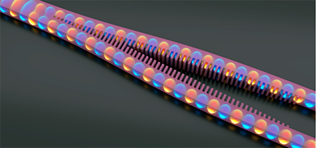
Integrated photonic circuits on the silicon-on-insulator (SOI) platform exhibit exceptional properties, including insensitivity to electromagnetic interference, small footprints, energy efficiency, and cost-effective large-scale production. Therefore, silicon photonics is a pivotal technology in telecommunications and data communication, expanding into high-impact emerging applications such as 5G mobile communications, biosensors, quantum computing, or artificial intelligence. Optical power splitters are a key component in any photonic chip, either to distribute light through the circuit or as a fundamental building block to construct more complex arrangements, but they typically operate in the C-band.
- Proposed solution
-
The designed ultra-broadband subwavelength metamaterial-assisted power splitter achieves efficient operation across a wavelength range covering all optical telecommunication bands: O, E, S, C, L and U (1260 nm - 1675 nm). Moreover, the device offers exceptionally low insertion loss (< 0.2 dB) for the entire wavelength range comprising these bands (O, E, S, C, L and U).
- Competitive advantages
-
- Unlike many state-of-the-art power dividers, which typically operate for a single optical mode, this device operates for three different modes: the fundamental and first-order transverse-electric (TE) modes, as well as the fundamental transverse-magnetic
- For TE modes, the device's operational bandwidth with minimal losses (< 0.1 dB) extends up to 2000 nm.
- The device has a compact design with a total length of less than 12 µm and robust manufacturing tolerances for all three modes.