- Stage of development
-
Prototype tested in laboratory
- Intellectual property
-
PCT application filed
- Intended collaboration
-
Licensing and/or co-development
- Contact
-
Patricia ThomasVice-presidency for Innovation and Transferpatricia.thomas@csic.escomercializacion@csic.es
- Reference
-
CSIC/PT/069
Additional information
#Materials
#Semiconductor
#Metals and alloys
#Chips / Circuits / Micro & nanoelectronics
Ultrathin films of van der Waals materials for electronic devices
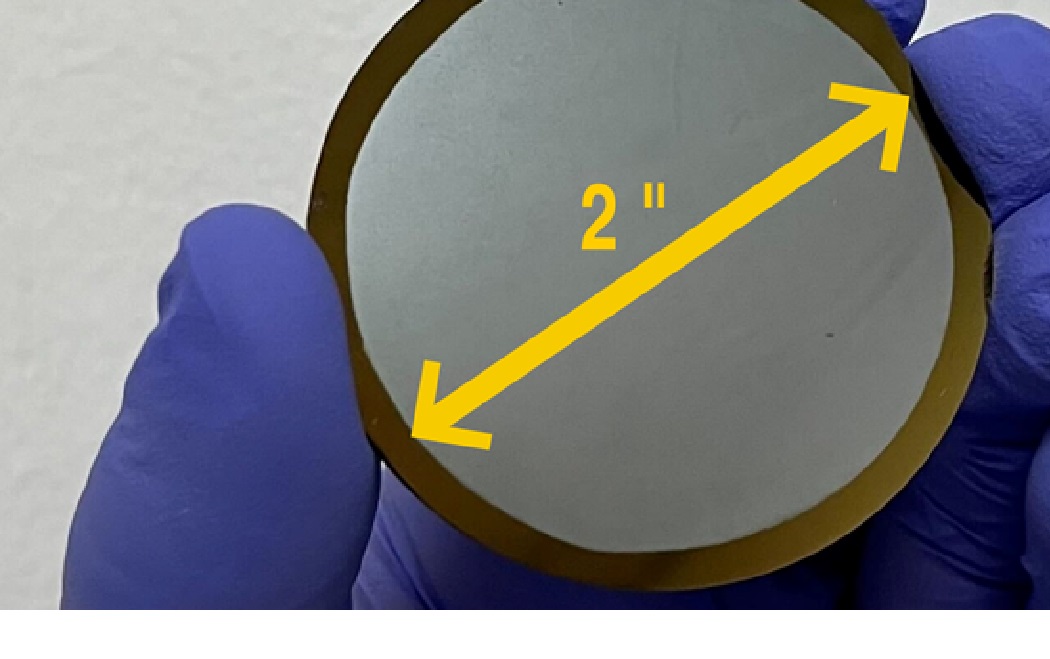
Semiconducting and metallic films were obtained through the novel Massive Parallel Mechanical Exfoliation of van der Waals materials. They consist of ultrathin nanosheets with a thickness ranging from a few atomic layers to several layers of material.
- Market need
-
Van der Waals materials excel in electronic and optoelectronic applications by maintaining high mobility even at sub-nanometric scales. Techniques like CVD, Mechanical Exfoliation or Liquid Phase Exfoliation are promising, but large-area production and reliable device fabrication remain challenging in terms of balancing complexity, costs, and features. These methods work well in labs but pose significant hurdles for large-scale manufacturing, highlighting a critical need for practical, scalable solutions.
- Proposed solution
-
This proprietary technology enables the production of van der Waals material films via Massive Parallel Mechanical Exfoliation. It involves a roll-to-roll procedure at adjustable speeds and pressures. The films consist of van der Waals overlapping nanosheets with thicknesses ranging from a few atomic layers to about 100 nm. This scalable process ensures high, uniform substrate coverage. It supports various materials, including graphite, molybdenite, BN, MoO3, WSe2, WS2, InSe, and black phosphorus, on substrates like Mylar, polycarbonate, or silicon wafers. There is a high yield in the production of batches of devices using this cost-effective technique.
- Competitive advantages
-
- Compared to liquid phase exfoliation, this dry method avoids solvent residues and offers enhanced dimensional control, producing flakes 10-100 times larger in lateral size involving less energy consumption.
- Compared to chemical vapor deposition (CVD), this technique simplifies the process and significantly reduces energy consumption, saving costs.
- The semiconducting film allows for the manufacturing of semiconductor devices, including photodetectors, sensors and transistors