- Stage of development
-
Device validated in laboratory
- Intellectual property
-
PCT application filed
- Intended collaboration
-
Licensing and/or co-development
- Contact
-
Alfonso del ReyVice-presidency for Innovation and Transferadelrey@icmab.escomercializacion@csic.es
- Reference
-
CSIC/AF/015
Additional information
#Energy
#Materials
#Renewable energy source
#Photovoltaics
#Measurement /sensing (materials)
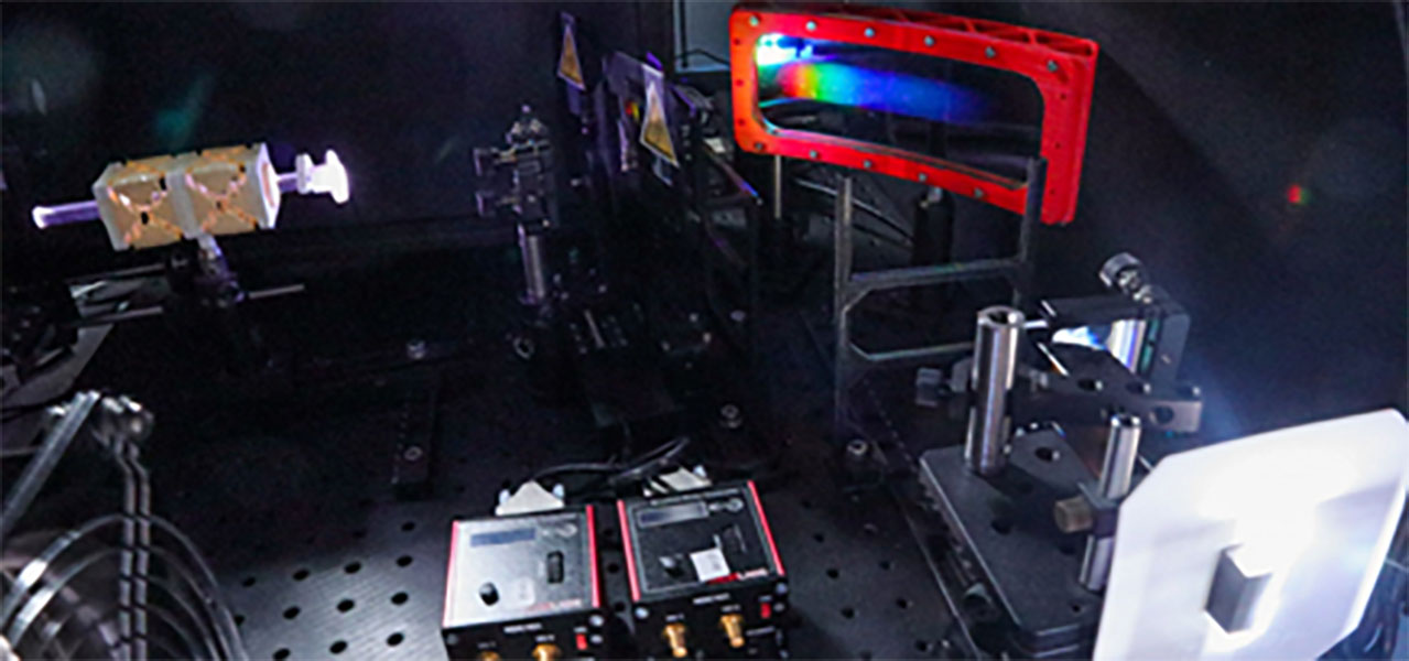
Spectral shaper illumination device
New illumination device suitable for optical spectroscopy characterization of optical and/or optoelectronic materials and devices
- Market need
-
In some applications, optical characterization may need a narrowband light source, while in others may need broadband illumination with a specific spectral distribution, and thus a plurality of pieces of equipment for a full characterization. For example, solar cell power conversion efficiency is characterized using a solar simulator with a broadband spectrum adjusted to outdoor sunlight or others, but external quantum efficiency is measured using monochromatic wavelength illumination.
- Proposed solution
-
An innovative device that provides a tunable, focused, spectrally Split beam, modulated in intensity and in a wavelength range with respect to the incoming light source. With this new device all the characterizations of optical and optoelectronic devices can be done with a single apparatus.
The apparatus works by spectrally splitting a broadband incoming light beam into its spectral components; then the beam passes a spatial filter stage which modifies the intensity of each colour separately; finally, the beam is condensed again providing either a rainbow spot (spatially separated colours) or a homogeneous spot with the desired spectrum at all loci.
- Competitive advantages
-
- Highly tunable light spectrum (spectrum on demand): from broad band (e.g. AM 1.5) to narrow band (up to FWHM of ca. 10 nm).
- Fast, computer aided modification of spectrum
- Enables novel characterization modes, such as optimization of tandem solar cells, advanced stability testing, etc.
- For applications in photovoltaic technologies, but also in solar thermal applications, photocatalysis, light degradation studies in materials, etc.